
Femtosecond (fs) laser micro/nano processing has emerged as a breakthrough technology enabling unprecedented precision in material modification, 3D structuring, and functional device fabrication. Its ability to deliver ultrashort laser pulses—shorter than the timescale of heat diffusion—allows truly “cold” machining with minimal thermal damage, enabling micro-scale features that conventional methods cannot achieve.
Femtosecond laser micro_nano pr…
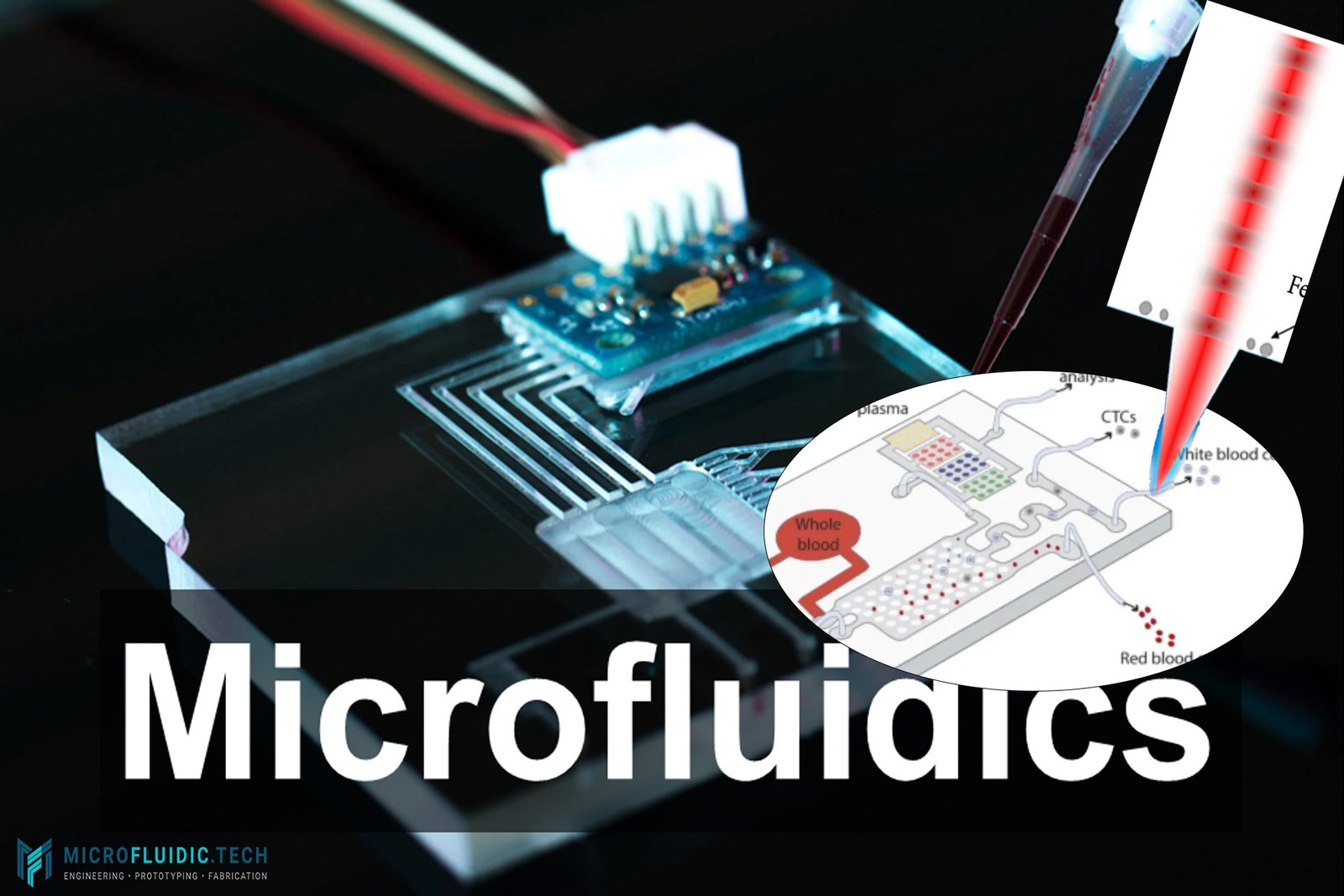
Over the past three decades, fs-laser technology has revolutionized fields such as microfluidics, lab-on-chip, biophotonics, micro-optics, and advanced manufacturing, giving researchers and industry new tools for next-generation devices.
Femtosecond laser micro_nano pr…
Why Femtosecond Lasers Matter in Microfluidics
Microfluidics thrives on precision. Channel smoothness, shape accuracy, and clean internal geometry directly affect flow behavior, mixing efficiency, and analytical performance. Traditional fabrication methods—photolithography, etching, and molding—come with constraints: multistep workflows, mask requirements, chemical waste, and limited 3D capability.
✔ True 3D Microchannel Fabrication Inside Transparent Materials
Fs-laser pulses can be focused deep within glass, polymers, or crystals to generate localized refractive index modification, nanogratings, or voids, enabling embedded microchannels, waveguides, and optical sensors.
✔ Minimal Heat-Affected Zone (HAZ)
Unlike nanosecond/ps lasers, fs-lasers avoid melting, cracking, and recast layers, producing clean channels and defect-free internal structures—critical for biological and chemical assays.
✔ Maskless, Direct-Write, Freeform Manufacturing
Design changes require no new masks. Complex 3D geometries, smooth curves, variable-depth channels, and multi-level networks are possible in a single step.
✔ Hybrid Integration of Functional Materials
Fs-lasers can integrate optical elements, electrodes, or sensors directly into microfluidic chips via localized modification, laser-assisted deposition, or two-photon polymerization.
Key Processing Capabilities Relevant to Microfluidics
1. Internal Microchannel Writing (Inside Glass / Polymers)
Using tightly focused femtosecond pulses, it is possible to inscribe channels beneath the surface, followed by selective wet etching or direct hollow formation. This allows:
-
enclosed microfluidic pathways
-
3D interconnected networks
-
hybrid micro-optic + microfluidic platforms
-
2. Surface Patterning for Wettability Control
Fs-laser ablation can create bio-inspired textures, such as lotus-leaf or moth-eye patterns, enabling:
-
superhydrophobic or hydrophilic surfaces
-
directional capillary flow
-
reduced sample adhesion
3. Drilling Through-Glass Vias & Ports
High-aspect-ratio hole drilling (aspect ratios up to 70+:1) can be achieved with GHz-burst fs-lasers—ideal for inlet/outlet ports, reservoirs, and through-substrate interconnects.
4. Two-Photon Polymerization for Microfluidic Add-ons
Two-photon polymerization (TPL) enables nanoscale 3D printing of:
-
valves
-
mixers
-
micro-grippers
-
micro-filters
-
optical elements embedded in channels
TPL offers sub-100 nm resolution—ideal for next-generation nanofluidic devices
Applications in Microfluidics & Lab-on-Chip
1. Integrated Optofluidic Chips
Waveguides, lenses, and microchannels can be fabricated monolithically, enabling real-time optical detection in microchannels.
2. Point-of-Care Diagnostic Devices
Fs-laser fabricated structures support high precision and high cleanliness—ideal for pathogen detection, chemical sensing, and biomarker screening.
3. Micro-bioreactors
Microstructures allow controlled environments for single-cell analysis, organ-on-chip, and cell culture studies.
4. High-Performance Micro-Needle and Nozzle Fabrication
Femtosecond processing enables low-roughness microscale holes beneficial for inkjet, drug delivery, and aerosol systems.
5. Quantum-Enabled Microfluidics
The creation of NV centers in diamond enables integrated quantum sensors for ultra-sensitive detection.
Advantages Over Conventional Microfabrication
| Feature | Fs-Laser Processing | Conventional Photolithography |
|---|---|---|
| 3D capability | ✔ True 3D, internal structures | ✖ Mostly 2D |
| Heat damage | Minimal (“cold ablation”) | Significant |
| Mask requirement | None | Required |
| Material versatility | Glass, polymers, crystals, diamond | Mostly silicon, glass |
| Resolution | Nano to microscale | Micro only |
| Hybrid integration | ✔ Optics, electronics, sensors | Limited |
This combination of precision, cleanliness, and design freedom is accelerating the transition toward high-performance, multi-functional microfluidic systems.
Future Outlook
Based on the recent review, the upcoming innovations include:
-
4D microfluidics using stimuli-responsive polymer printing
-
heterogeneous material integration (optics + electronics + fluidics)
-
AI-optimized laser path planning for higher throughput
-
ultrafast nanocrystal printing for sensing and photonic integration
As fs-laser systems become more affordable and industrially scalable, they are poised to become a standard tool in advanced microfluidics manufacturing.